We have carried out the development and the associated manufacturing of (1) metallic and ceramic thin film / nanocoating for RF applications, (2) RF nanocomposites.
Presently we are developing and commercializing a spin-spray deposition process. It is a novel class of low-cost, scalable process that can directly synthesize/deposit a crystalline spinel ferrite film with various compositions directly from an aqueous solution with a low processing temperature between 25– 90 °C. The approach of spin-spray deposited ferrites has provided great opportunities to achieve a low-temperature synthesis of a single ferrite materials or multiferroic composite materials on ferroelectric substrates or flexible polymer substrates for lightweight, small-size antenna applications.

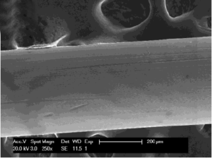
Over years we have successfully developed a novel class of low-cost, scalable process, nano-coating technology to synthesize metallic nanocoatings on carbon/graphite micro/nanofibers and carbon nanotubes and graphene. This nano-coating technology based on a modified electroless coating is expected to offer the advantages such as high processing efficiency, good processing consistency, and low processing cost, which is also scalable for large-quantity production and applicable for carbon nanofibers/tubes with different diameters/lengths.
We have also developed novel class of ceramic nanocoating technology to generate high-temperature, electrically-insulating (HTEI) nanocoating for copper magnet wires, which would enable the power conversion systems to operate at higher power densities, high temperatures and high frequencies. This coating technology based on the pyrolysis of polyceramic precursors is expected to offer advantages such as high efficiency, small size and light weight for resultant power electronic components and power conversion systems. The processes developed will also be scalable for large-quantity production and applicable for copper wires with different diameters.
Bioenno also provides the service of nanoimprint lithography, a method of fabricating nanometer scale patterns. This processing technology, which is a simple nanolithography process with low cost, high throughput and high resolution, creates patterns by mechanical deformation of imprint resist and subsequent processes. Nanoimprint lithography has been used to fabricate devices including various sensors and detectors for electrical, optical, photonic and biological applications. In addition, Bioenno Tech has carried out the development of semiconductor quantum dots (QDs) for IR sensors and other detector applications such as using inorganic colloidal quantum dots in the visible wavelength range as the fluorescent penetrant for nondestructive examination of surface flaws