Over years Bioenno Electronics has conducted extensive development directed toward the commercially viable products of (1) Optical modulators for telecommunications, (2) Photodetectors, and (3) IR sensors, based on the following technology development:
1. Optical Modulator
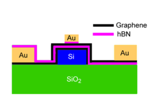
We have built on extensive experiences in the designs and development of optical modulators, by utilizing our highly capable hybrid packaging technology. Currently we are developing a novel class of graphene-based optical modulators — A high-speed, broad-range, small-foot print, low-cost graphene based optical modulator. These recent investigations have suggested the graphene-based optical modulator would open a new promising path for next-generation optical communication. As compared with traditional devices, the graphene-based optical modulator would be able to work at a few hundred of gigahertz, much faster than the present integrated devices currently limited to 40GHz. It can work at a broad spectrum of wavelength, ranging from 400 nm up to far-infrared, while the range of other devices is from a few picometers to nanometers. Also, its small footprint (tens of microns) also offers the potential for this class of modulator to be easily integrated. In addition, the price of the device could potentially be low. All those combined features would make the graphene-based modulator a device that is promising for optical interconnects in future integrated optoelectronic communication system and expected to address a major portion of the optical modulator market. Despite these promising advantages demonstrated, more studies and developments addressing the design and manufacture of graphene-based optical modulators directed toward a commercially viable product are anticipated before the full potential can be achieved. In this project, Bioenno Tech is to develop a novel class of graphene-based optical modulators that can be used for optical communication, with higher modulation speed, broader bandwidth, smaller footprint and lower costs over conventionally available optical modulators.
The major features of this development and the resultant graphene-based modular include: (1) A novel design of graphene-based modulator with anticipated 3dB bandwidth of up to ~200 GHz ( much larger than the present integrated devices with a record speed of 40 GHz), which can be fabricated with a well-established, low-cost micro-fabrication process, (2) Low insertion loss of ~1dB and high modulation depth of ~0.6, and (3) Working at a broad wavelength range from 400nm to 4µm.
Besides enhanced performance, the proposed modulators will also offer the following advantages: (1) Enhanced compatibility with silicon photonic systems compared with conventional devices, (2) Lower costs based on inexpensive graphene manufacturing methods compared with an epitaxial process employed in conventional technology, and (3) High density integration with a compact size for optical interconnects in intra- and inter-chip communication links due to the ultrathin structure of graphene, allowing for monolithic integration with silicon photonic systems.
2. Photodetectors
We have built on extensive experiences in the designs and development of photodetectors, by utilizing our highly capable hybrid packaging technology. One is ZnO based UV photodetectors for the solar-blind detection window. Detection of ultraviolet (UV) has been used in many fields, such as flame sensors, detectors of high energy physical particles and space-to-space communication. UV photodetectors (PDs) based on the wide bandgap semiconductors, such as SiC, GaN, and ZnO have been widely used in the above applications, in spite of some disadvantages such as high cost and complicated fabrication process.
This project is to develop and demonstrate (1) (Be,Mg)ZnO semiconductor alloys of high optical quality with optical bandgap of approximately 280 nm for solar blind detection regime, (2) The associated demonstrate doping and contact formation needed for the complete UV photodetector; and (3) Final prototypes of high-responsivity solar-blind photodetectors (265-280 nm) that can be standard p-n junction photodetectors or avalanche photodetectors, with the performance goals surpassing current SBDs with approximate photoresponse of 200 mA/W.
The potential applications include: (1) UV non-line of sight (NLOS) optical communications, bio-warfare agent detection, missile detection from plume signatures, and other spectroscopic UV signatures; and (2) Biosensing and bio-agent detection, flame detection, determination of engine combustion efficiency, atmospheric ozone studies, and astronomical studies.
Our current focus is on performance enhancement of MgZnO and MgBeZnO based solar blind UV detectors, addressing related issues with doping and miscibility, which involve the use of advanced sputtering growth techniques and consideration of both Schottky and p-n junction devices. Novel doping strategies as well as the use of nearly lattice matched oxide substrates will be explored, which is also accompanied with optimization of device design with the aid of simulation software. The prototype of detector which will be robust and compact, will be fabricated to demonstrate the feasibility of the technology, and the final devices can be sought as replacements for photomultiplier tubes (PMTs) in current use. The resultant ZrO2-based MSM UV photo detectors will have lower fabrication costs and also provide a robust and compact alternative to bulky photomultiplier tubes, for sensitive and fast detection of UV light for many applications. This technology will be used in a number of fields, such as solar UV monitoring, high energy physical particles, flame sensor, and biological research, as well as in UV astronomy and secure space-to-space communication.
3. IR Sensors/Detectors
One recent project is Quantum-dot Based Infrared Detectors and Infrared Focal Plane Array. In this project, Bioenno Tech proposes to develop a middle/long-wave infrared (LWIR) focal plane array (FPA) based on chalcogenide semiconductor quantum dots (QDs) such as GeTe@PbTe and SnTe@PbTe QDs. Instead of III-V materials whose composition and particle shape are hard to control, chalcogenide-based QDs are advantageous in particle shape and superstructure control that are better in achieving constant properties for potential processing scale up and commercial applications. The resultant QD-based LWIR FPA will provide the advantages of high-efficiency, high-sensitivity, and lower costs over currently available IR detectors using conventional technologies.
